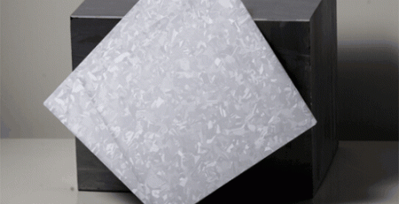
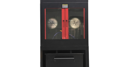
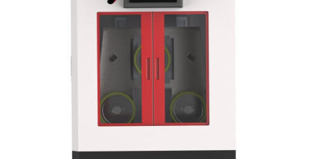
결정질 실리콘 잉곳 절단 방법
청정 에너지의 급속한 발전과 함께, 태양광 발전을 위한 그리드 패리티(Grid Parity)의 목표도 임박했습니다. 태양광 산업의 다양한 결정질 실리콘 제조업체는 지속적으로 생산 능력을 확장하고 있습니다, 또한 지속적으로 생산 비용을 절감하고 있습니다, 작은 실리콘 잉곳의 절단은 결정질 실리콘 태양 전지 비용의 중요한 구성 요소입니다.
- 결정질 실리콘 잉곳은 내경 블레이드, 슬러리 와이어 톱 또는 고정 다이아몬드 와이어 루프로 절단할 수 있다; 다이아몬드 와이어가 현재 주된 방법이다.
- 고정 연마 다이아몬드 와이어는 느슨한 연마 슬러리 절삭보다 더 좁은 케르프와 더 나은 표면을 생성한다, 슬러리를 관리할 필요가 없다.
- 연구와 생산 데이터 모두 다이아몬드 와이어 루프 절단이 케르프 손실을 줄이고 태양광용 실리콘 수율을 높인다는 것을 보여준다.
아래 방법들은 모두 실리콘 웨이퍼 절단, 케르프 손실과 TTV가 최종 잉곳당 수율을 결정하는 곳으로 연결된다.
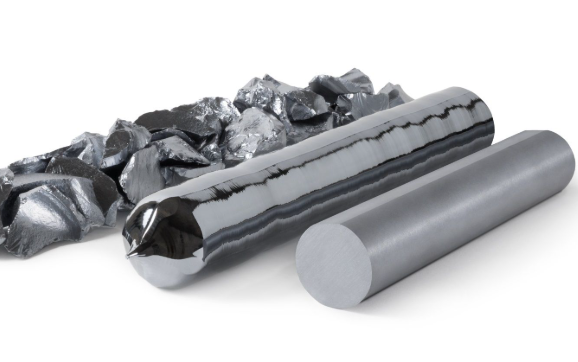

실리콘 잉곳이란 무엇인가?
결정질 실리콘 잉곳은 큰, 원통형 (또는 준정사각형) 단결정 또는 다결정 실리콘 막대로 규칙적인 원자 배열을 가진 것이다, 고순도 폴리실리콘 원료를 용융시키고 정밀하게 제어된 결정 성장 기술을 사용하여 생산됨. 실리콘 웨이퍼 제조를 위한 직접적인 전구체 재료로 사용됨.
예외적으로 높은 순도: 실리콘 공급 원료는 일반적으로 최소한의 순도 수준을 달성해야 하며 99.9999% (6N), 반도체 등급 실리콘은 최대 순도가 필요함 99.999999999% (11N). 이러한 극도로 낮은 불순물 함량은 우수한 전기적 특성을 보장하는 데 필수적임.
완벽한 결정 구조:
- 단결정 실리콘 잉곳: 전체 잉곳은 결정립 경계가 없는 완전히 균일한 원자 방향을 나타냄. 이 구조는 매우 높은 변환 효율과 우수한 전기적 성능을 제공함, 이로 인해 단결정 실리콘은 고효율 태양광 전지와 첨단 반도체 칩의 절대적인 주류 재료가 됨.
- 다결정 실리콘 잉곳: Composed of numerous silicon grains of varying sizes separated by grain boundaries. While production costs are relatively lower, the conversion efficiency and electrical performance are slightly inferior to those of monocrystalline silicon.
Trend Toward Larger Dimensions: To enhance production efficiency and reduce downstream costs, the diameter of silicon ingots continues to increase. 현재, mainstream solar-grade 단결정 실리콘 ingots have reached diameters of 210mm (G12) or larger, while semiconductor-grade ingots commonly correspond to wafer sizes of 200mm (8 인치) and 300mm (12 inc
다이아몬드 절단 와이어 루프가 결정질 실리콘 절단에 사용되는 이유
태양 에너지 신청을 위한 crystalline 실리콘 주괴를 자르기의 과정에서, 대부분의 제조업체는 현재 절단을 위해 강선 및 모르타르와 함께 전통적인 다이아몬드 톱날을 사용합니다. 다이아몬드 톱날은 절단 속도가 빠르지만 넓은 절단을 생성합니다. 절단 과정에서, 많은 양의 실리콘 재료가 면도되어 폐수로 들어가는 실리콘 분말로 만들어집니다, 그 결과 높은 실리콘 손실이 발생합니다..
The silicon consumption of 다이아몬드 커팅 와이어 루프 cutting lines is one-third that of diamond saw blade cutting lines, 상당한 실리콘 재료 절약 가능. 강선과 모르타르를 사용하는 절단 방법이 느립니다., 그리고 모르타르와 실리콘 분말은 모두 폐수에 함께 들어갑니다. 그것들을 분리하는 데 드는 비용이 높습니다, 상당한 양의 모르타르를 회수해야 합니다., 환경에 악영향을 미침. 또한, 폐수 처리 비용이 높습니다..
다이아몬드 절단 와이어 루프의 절단 속도는 다음과 같습니다. 2-3 모르타르 및 강선 절단 방법보다 빠른 시간, 그리고 생산된 실리콘 분말은 수성 냉각액과만 혼합됩니다, 결과적으로 폐수 처리 비용이 절감됩니다.. 결정질 실리콘 잉곳을 절단하기 위해 다이아몬드 절단 와이어 루프를 사용하여, 고속 절단, 환경 친화성, 그리고 저가 생산은 달성될 수 있습니다.
다이아몬드 화강암 와이어 톱의 현재 개발 상태.
전기도금을 한 다이아몬드 절단 와이어는 결정질 실리콘 잉곳 절단에서 강력한 절삭력과 깔끔한 절단 이음새와 같은 장점이 있습니다, 지난 3년 동안 급속한 발전을 경험했습니다.. 그것은 광전지 산업에서 널리 사용되었을 뿐만 아니라 사파이어 및 자성 재료 절단과 같은 다른 분야에서도 사용되었습니다.
그렇지만, 전기 도금 된 다이아몬드 절단 와이어의 생산에는 여전히 문제가 있습니다, 불안정한 프로세스와 같은, 다이아몬드 입자의 쉬운 분리, 그리고 높은 생산 비용, 전기 도금 된 다이아몬드 절단 와이어의 광범위한 채택을 방해하는지.
다이아몬드 와이어 루프에 대한 연구 결과.
복합 전기 도금의 기본 이론을 기반으로, 이 기사에서는 다이아몬드 절단 와이어 루프의 전기 도금에 영향을 미치는 공정 매개 변수를 조사합니다. 실험에서, 0.27mm 직경의 동도금 고탄소강선을 기본선으로 사용했습니다. 전기 도금 용액은 니켈 설파메이트 전기 도금 용액을 사용했습니다, W30-40 다이아몬드 입자가 사용되었습니다.. 니켈 도금을 이용한 다이아몬드 입자의 전처리에 관한 결론이 도출되었습니다, 화학 니켈 도금 방법으로 절단 목적으로 전기 도금 된 다이아몬드 절단 와이어 루프를 생산하는 데 가장 적합한 것으로 밝혀졌습니다.. 니켈 도금 다이아몬드 입자의 중량 비율의 다양한 매개 변수 연구를 통해, 니켈 도금된 다이아몬드 입자에 대한 안정적인 생산 중량 비율이 결정되었습니다..
설파메이트로 전기도금을 하는 니켈의 전류 밀도가 코팅의 취성에 미치는 영향을 연구함으로써, 전기도금을 한 다이아몬드 절단 와이어 루프를 생산하기 위한 최적의 전류 밀도가 확인되었습니다.. 설파메이트 니켈 전기 도금의 두께가 전기 도금 된 다이아몬드 절단 와이어 루프의 절단 성능에 미치는 영향을 조사함으로써, 니켈 도금층에서 다이아몬드 입자의 최적 매몰률을 결정하였다.
단위 면적당 다이아몬드 입자 수가 전기 도금 된 다이아몬드 절단 와이어 루프의 절단 성능에 미치는 영향을 연구함으로써, 절단을 위한 다이아몬드 와이어 루프 절단을 위한 최상의 성능에 해당하는 단위 면적당 최적의 다이아몬드 입자 수가 결정되었습니다.. 전기 도금 된 다이아몬드 절단 와이어 루프의 절단 효율에 대한 응력 제거 온도 및 시간의 영향을 조사함으로써, 최적의 응력 제거 매개변수가 식별되었습니다.. 결국, 결정질 실리콘 잉곳을 절단하기 위한 전기도금을 한 다이아몬드 절단 와이어 루프의 산업 생산이 이루어졌습니다..
자주 묻는 질문
What methods are used to cut crystalline silicon ingots?
The three historical methods are inner-diameter blade saws, loose-abrasive slurry wire saws and fixed diamond wire loops. 다이아몬드 와이어 루프 절단이 주류 선택이 되었다.
왜 다이아몬드 와이어 루프가 슬러리 쏘잉보다 선호되는가?
고정 다이아몬드 연마재는 더 좁은 절단선을 제공한다, 슬러리 취급이나 폐기 없이 더 깨끗한 공정, 주괴당 더 많은 웨이퍼.
결정성 실리콘 주괴란 무엇인가?
Czochralski와 같은 방법으로 성장한 단결정 또는 다결정 실리콘 실린더, 그 후 태양전지와 반도체 소자용 웨이퍼로 절단된다.
엔솔 엔지니어링 팀이 검토한 기술 내용 — 다이아몬드 와이어 루프 제조업체 10+ 다년간의 생산 경험을 가진 회사.