산업 뉴스

Industry news and market insights on diamond wire cutting, precision machining and advanced materials.

Cutting Methods for Crystalline Silicon Ingots

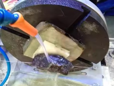
청정 에너지의 급속한 발전과 함께, 태양광 발전을 위한 그리드 패리티(Grid Parity)의 목표도 임박했습니다. 태양광 산업의 다양한 결정질 실리콘 제조업체는 지속적으로 생산 능력을 확장하고 있습니다, 또한 지속적으로 생산 비용을 절감하고 있습니다, 작은 실리콘 잉곳의 절단은 결정질 실리콘 태양 전지 비용의 중요한 구성 요소입니다. Key Takeaways Crystalline silicon ingots can be cut with inner-diameter blades, slurry wire saws or fixed diamond wire loops; diamond wire is...
사파이어 커프 폐기물 재활용: 연구

핵심 내용: 사파이어 웨이퍼 두께는 약 0.2 mm로, 다이아몬드 와이어 직경과 비슷하며, 대략 40-50% of every ingot becomes cutting-waste powder washed away by coolant, and most of it has historically been landfilled. Analysis of washed, dried and sieved diamond-wire cutting waste shows alpha-alumina as the main component, with nickel (0.70%) and diamond (0.164%) as the main impurities. Ultrasound acid leaching beats conventional acid leaching for nickel removal: nickel falls to 0.009% at a 99.67% leaching ratio, 그리고...

Resin Hardness vs Diamond Wire Loop Performance

추상적인: 이 연구는 다이아몬드 와이어 루프의 절단 성능에 대한 다양한 수지 바인더의 영향을 조사합니다. 수지 경화 경도 샘플은 순수 페놀 수지를 사용하여 준비되었습니다, 에폭시 변성 페놀 수지, 및 방향족 알킬 변성 페놀 수지, 그리고 그들의 로크웰 경도가 시험되었습니다. 경화된 수지 샘플의 파괴된 표면은 주사 전자 현미경을 사용하여 관찰되었습니다, 경화 후 다양한 수준의 밀도 표시. 그런 다음 다이아몬드 와이어 루프를 단결정 실리콘 절단 실험을 위해 제조했습니다. 실험 결과는 다이아몬드 와이어 루프가 만들어졌음을 보여줍니다..

Best Cutting Method for KDP Crystals

KDP 크리스탈 소개 KDP 크리스탈은 비선형 광학 계수가 크고 레이저 손상 임계값이 높습니다, 고에너지 엔지니어링을 위한 광학 시스템의 중요한 구성 요소로 만들기. KDP 결정은 가공하기 어려운 부서지기 쉬운 재료에 속합니다., 전통적인 금속 재료 가공과 구별. KDP 크리스탈의 제조 공정 제조 공정에는 대략적인 모양으로 절단한 다음 정밀 절단하는 작업이 포함됩니다. 절단은 KDP 크리스탈 재료 가공의 첫 번째 단계입니다. 크리스탈 블랭크의 국부적인 응력으로 인해, 전체 크리스탈...

Cutting Fluid Impact on Diamond Wire Loop Quality

절삭유가 다이아몬드 와이어 루프의 절삭 품질에 미치는 영향을 고려할 때, 몇 가지 요인이 작용합니다. 절삭유의 선택은 절삭 공정의 효율성과 효과에 큰 영향을 미칠 수 있습니다. 고려해야 할 몇 가지 측면은 다음과 같습니다: 절삭유의 개념: 절삭유, 절삭유 또는 절삭유라고도 합니다, 유성 및 수성 형태로 제공됩니다., 청소와 같은 다양한 목적으로 사용, 윤 활, 그리고 기계로 가공 과정 도중 냉각. 이러한 유체는 유지 관리에 매우 중요합니다...

단결정 실리콘 잉곳 가공 흐름

주요 요점: 단결정 실리콘 잉곳은 크롭핑을 거칩니다, 직경 연삭, 깔 끔 히, 모서리 모서리 캐핑, lapping and polishing before it is ready for lithography. Surface accuracy at the slicing stage determines how much downstream planarization work is required. Diamond wire slicing is the standard way to turn an ingot into bare wafers with tight thickness variation and low sub-surface damage. 단결정 실리콘 웨이퍼 준비 단계에서, the silicon single-crystal ingots need to be processed into raw silicon wafers or barewa-fers with high surface accuracy...

다양한 반도체: 유형과 응용

What is a Semiconductor A semiconductor chip, 일반적으로 집적 회로라고 합니다, is a semiconductor device fabricated on a semiconductor wafer through processes such as etching, wiring, and patterning to achieve specific functions. Beyond silicon chips, common semiconductor materials include gallium arsenide, 질화갈륨, and silicon carbide. Key Takeaways Semiconductors are materials with conductivity between conductors and insulators, forming the basis of all integrated circuits. Beyond silicon, key semiconductor types include gallium arsenide (가스(GaAs)), 질화갈륨 (질화 갈륨) and silicon carbide (원문대로), each...

반도체의 이해: Origins Explained

Key Takeaways A semiconductor is a material with properties between an insulator and a conductor, controllable through doping and electric fields. Understanding semiconductors evolved from early crystal detectors to the transistor and today's integrated circuits. This controllable conductivity is what makes all modern electronics possible. 반도체란?? 간단히 말해서, a semiconductor is a material that exhibits properties between an insulator and a conductor. Insulators are materials that do not conduct electricity, while conductors are materials that conduct electricity. Semiconductors possess characteristics that lie...