실리콘 카바이드 절단: 다이아몬드 와이어 톱 가이드
고급 반도체의 까다로운 세계에서, 성능과 효율성이 최우선인 곳에서, 한 가지 재료가 중요한 촉매 역할을 합니다.: 실리콘 카바이드 (원문대로). Known for its exceptional hardness (second only to diamond), 높은 열전도율, and superior electrical properties, SiC is the cornerstone of next-generation power electronics. 그렇지만, its very advantages make it notoriously difficult to process. This is where the transformative power of the 다이아몬드 와이어 톱 comes into play, acting as the scalpel that unlocks the potential of this super material.
- Silicon carbide ranks about 9.2–9.5 on the Mohs scale — close to diamond — and combines that hardness with brittleness, so blade and laser cutting both leave damage.
- Diamond wire is the matching tool: S, i.
- C 20 SiC의 가장자리 칩 μm. 다이아몬드 와이어는 칩을 거의 0에 가깝게 유지, 이 차이가 전력 장치와 RF 칩의 수율을 보호한다.
- 생산 중, SiC MOSFET에서 레이저에서 다이아몬드 와이어로 전환하면 수율이 상승 78% 받는 사람 93% at 500 mm/min — 이득은 거의 전적으로 균열로 인한 고장을 제거함으로써 나왔다.
- 와이어는 다음과 같이 미세하게 작동할 수 있다 0.2 밀리미터. SiC 불은 비싸기 때문, 좁은 절단선이 결정당 더 많은 웨이퍼로 변환된다.
- SiC/GaN 작업의 경우, 직경 0.1–0.3mm의 와이어와 10–20 μm 다이아몬드 그릿을 지정, 기계 진동을 그 이하로 유지 0.1 μm — 입자가 재료를 절단한다, but vibration is what creates the micro-cracks.
- GaN은 SiC와 다르게 고장난다: 그것은 덜 단단하지만 높은 파괴 인성을 가진다, 그래서 마모되기보다는 금이 간다. 저진동 와이어 절단이 GaN에서는 원재 연마 경도보다 더 중요하다.
SiC 도전: 길들이기 어려운 재료
SiC가 효율적인 전기차 인버터나 소형 전력망 컨버터의 핵심이 되기 전에, 단단한 불을 얇은 웨이퍼로 정밀하게 절단해야 한다. 전통적인 절단 방법, 예를 들어 연마 슬러리 톱들은, SiC 처리에 어려움을 겪는다. 그들은 느리다, 상당한 폐기물을 생성한다, 그리고, 가장 중요한 것은, 취성 결정에 미세 균열과 높은 응력을 유발한다. 이러한 결함은 성능 저하를 일으키며, 최종 칩의 수율과 신뢰성을 낮춘다. 업계는 SiC의 경도와 동일한 정밀함과 섬세함을 가진 솔루션을 필요로 했다.
 Why Diamond Wire Saw is the Perfect Match for SiC
The diamond wire saw operates on an elegantly simple yet profoundly effective principle: a continuous loop of steel wire, electroplated with diamond particles, moves at high speed to perform a clean, linear cut. For SiC, this technology offers a suite of unbeatable advantages:
- Minimized Kerf Loss, Maximized Yield: The diamond wire can be incredibly thin (as fine as 0.2mm). This creates an extremely narrow cut path, or “kerf.” Given the high cost of SiC boules, every millimeter saved translates directly into more wafers per crystal and substantial material cost savings. This efficiency is fundamental for making SiC technology more commercially viable.
- Superior Surface Integrity: The continuous, controlled cutting action of the wire generates minimal mechanical and thermal stress. The result is a wafer surface with exceptional as-cut quality—smoother and with dramatically fewer micro-cracks compared to traditional methods. This “low-damage” surface means the subsequent, time-consuming grinding and polishing steps can be significantly reduced, accelerating the entire production workflow.
- Uncompromised Crystal Quality: Perhaps the most critical advantage for semiconductor applications is the preservation of SiC’s intrinsic electrical properties. The clean, low-stress cut ensures the crystalline lattice at the wafer’s edge and surface remains intact. This directly contributes to higher chip performance, better breakdown voltage characteristics, 그리고 궁극적으로, more reliable and powerful electronic devices.
- Cool and Controlled Processing: The cut is typically performed with a water-based coolant, preventing localized overheating that could alter the material’s properties. This “냉 절단” process is essential for maintaining the precise stoichiometry and quality required for high-end semiconductors.
From Wafer to Wonder: The Journey of a Cut SiC Wafer
Once sliced and polished, these pristine SiC wafers become the foundation for a technological revolution. Their primary destination is the fabrication of power semiconductor devices
- Electric Vehicles (EVs): SiC MOSFETs and diodes form the core of the main traction inverter. They switch electricity with far less loss than traditional silicon chips, enabling longer driving range, faster charging, and more compact, efficient powertrains.
- 재생 에너지: In solar inverters and wind turbine converters, SiC devices handle high voltages and frequencies with exceptional efficiency, 녹색 전력이 전력망에 공급되는 에너지 손실 최소화.
- 5G & RF 인프라: SiC의 고주파 능력은 차세대 통신 기지국의 무선 주파수 증폭기에 이상적, 더 빠른 데이터 전송 가능하게 한다.
- 산업용 모터 구동장치: SiC 기반 드라이브는 더 작게 만들 수 있다, 산업용 모터의 제어 시스템 효율, 제조 및 자동화 시 에너지 절감 효과.
다이아몬드 와이어 톱의 경도와 특성 이해
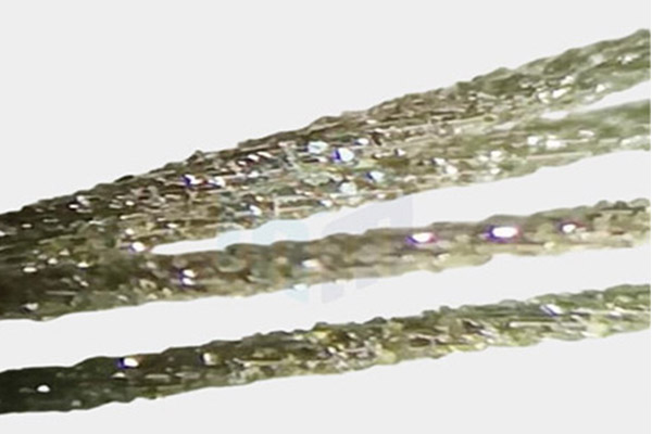
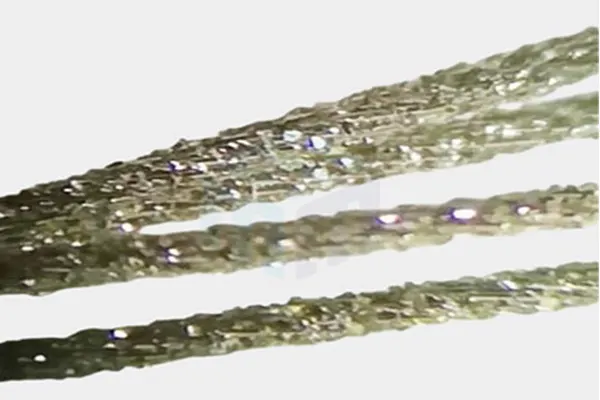
- 다이아몬드 와이어 톱의 경도는 와이어에 내장된 다이아몬드 입자에 기인합니다. 다이아몬드는 뛰어난 경도로 유명합니다, 가장 단단한 자연 발생 물질로 선정. 와이어 톱에 통합될 때, 다이아몬드는 다양한 재료를 쉽게 관통하고 연마할 수 있는 우수한 절삭날을 제공합니다.
탄화규소의 경도와 특성에 대한 이해
탄화실리콘 절단 시 도전
1. 극심한 경도 및 취성:
모스 경도가 대략 그대로 9.5, 다이아몬드와 질화붕소에 이어 두 번째, SiC는 매우 단단하고 취성성이 강한 재료. 기존 절단 도구는 빠르게 마모되며, 비용 효율 저하. 더 중요한 점은, 취성으로 인해 미세 균열에 매우 취약하다, 가장자리 칩핑, and subsurface damage during mechanical cutting. This damage layer can severely degrade the performance and reliability of the final semiconductor device.
마지막 리뷰: 9월 2026
2. Low Cutting Efficiency and High Tool Wear:
Using diamond tools (such as diamond wire or blades) is almost mandatory. 그렇지만, even diamond abrasives experience substantial wear when cutting SiC, leading to decreasing cutting rates over time, increased heat generation, and higher consumable costs. The process often requires multiple steps (roughing and finishing) to achieve the desired surface integrity, further reducing overall throughput.
3. Demands for Ultra-High Precision and Surface Quality:
Semiconductor wafers require exceptional geometric accuracy (nanometer-level flatness and thickness uniformity) and a damage-free, ultra-smooth surface. Any micro-cracks or subsurface stress introduced during cutting must be minimized, as they can propagate during subsequent grinding and polishing steps, causing wafer breakage or defective devices. Achieving this while maintaining high yield is a major hurdle.
4. Thermal Management and Stress Control:
The cutting process generates significant localized heat. SiC’s high thermal conductivity helps, but if not managed properly, thermal stress can exacerbate cracking or alter material properties. Effective cooling (often using specialized coolants) and precise control of cutting parameters are crucial to prevent thermal damage.
5. High Cost of Processing:
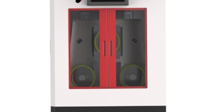
The combination of expensive diamond tools, slow cutting speeds, the need for sophisticated equipment (like multi-wire saws or laser-assisted systems), and strict cleanroom environments contributes to very high manufacturing costs for SiC wafers. This remains a key factor limiting its broader adoption.
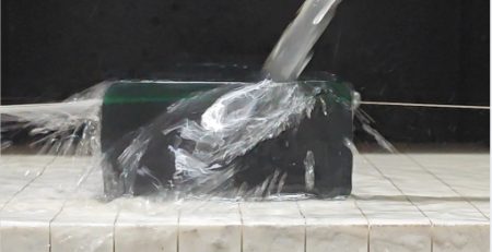
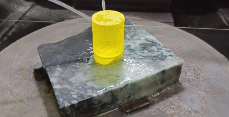
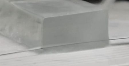
비디오 쇼케이스:
사례 연구: SiC 파워 모듈 생산
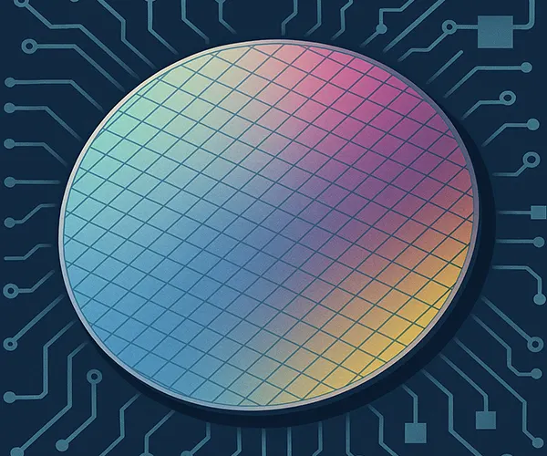
- 결과 1: 수확량이 에서 증가했습니다. 78% 받는 사람 93%(균열로 인한 고장 감소).
- 결과 2: 절단 속도 도달 500mm / 분0.3μm 다이아몬드 와이어 포함
올바른 다이아몬드 와이어 톱 선택
SiC/GaN 애플리케이션용, 우선 순위:
- 와이어 지름: 0.1미세 마감의 경우 –0.3mm.
- 다이아몬드 그릿 크기: 10속도와 표면 품질 사이의 균형을 위한 –20μm.
- 기계 안정성: 진동 <0.1μm로 미세 균열 방지.
미래 트렌드
- 하이브리드 절단: 다이아몬드 와이어와 레이저 사전 홈 가공을 결합하면 이기종 통합.
- AI 기반 프로세스 제어: 에 대한 실시간 조정 결함 없는 절단.
결론: Cutting the Path to the Future
The diamond wire saw is far more than just a cutting tool for Silicon Carbide; it is a critical enabling technology. By providing a means to slice this ultra-hard material with unparalleled precision and care, it directly supports the advancement of technologies that are making our world more electrified, connected, and energy-efficient. As demands for SiC wafers grow in both size and quantity, the evolution of diamond wire technology—towards even finer wires, smarter tension control, and higher throughput—will continue to be essential in powering the sustainable, high-tech future.
자주 묻는 질문
실리콘 카바이드를 자르기에 가장 좋은 도구는 무엇인가요??
다이아몬드 와이어 톱. SiC는 경도에서 다이아몬드와 가깝기 때문에, 다이아몬드 연마재만이 효율적으로 절단할 수 있습니다, 와이어의 연속적 저압 작용은 블레이드와 레이저가 일으키는 부스러기 및 열 영향 손상을 피할 수 있습니다.
실리콘 카바이드를 자르기 어려운 이유는 무엇인가요??
모스 경도 약 9.2–9.5와 깨지기 쉬운 특성: 기계적 힘은 가장자리를 다치게 하고 레이저 열은 미세 균열을 유발합니다. 어떤 방법을 선택하든, 두 가지 실패 모드 중 하나는 반드시 설계 과정에서 제거해야 합니다.
레이저 절단이 SiC에 손상을 주나요??
예. 레이저 제거는 열 영향층과 다시 용융된 층을 남기며, 이는 연마해야 하므로, 비용과 수율 손실이 발생합니다.
블레이드 다이싱이 SiC에 남기는 가장자리 부스러기는 어느 정도인가요??
일반적인 블레이드 다이싱은 일반적으로 더 큰 가장자리 결함을 생성합니다 20 μm의. 전력 장치와 RF 칩에서 칩이 직접적인 항복 손실을 초래한다, 이것이 팹들이 다이아몬드 와이어로 전환하는 주된 이유.
다이아몬드 와이어가 SiC 레이저 절단보다 어떤 수율 향상을 가져올 수 있는가?
SiC MOSFET의 레이저 절단에서 다이아몬드 와이어 절단으로 전환된 SiC 전력 모듈 라인에서, 수율이 상승했다 78% 받는 사람 93% 작동 중 500 mm / 분. 개선은 더 빠른 절단이 아니라 균열로 인한 파손을 제거함으로써 나왔으며.
다이아몬드 와이어 쏘가 갈륨 질화물을 절단할 수 있는가 (질화 갈륨) 웨이퍼?
예, 공정 창이 SiC와 다르다. GaN은 경도는 낮지만 파괴 인성이 높으며, 공구 마모보다는 미세 분열이 일어나는 경향이 있다. 미세 와이어를 사용, 중간 정도의 그래트와 매우 낮은 기계 진동 — 이하 0.1 μm — 표면 아래 균열을 방지하기 위해.
다이아몬드 와이어가 SiC에서 어떤 표면 마감을 달성할 수 있는가?
가는 와이어와 안정적인 장력으로, 서브 마이크론 Ra가 달성 가능하며 — 종종 연마 단계를 완전히 줄이거나 제거함.
SiC를 절단할 때 커프는 얼마나 얇을 수 있는가?
다이아몬드 와이어는 매우 가늘게 운용될 수 있으며 0.2 밀리미터, 매우 좁은 절단 경로를 제공함. SiC 부울의 비용을 고려할 때, 절약된 밀리미터마다 결정당 더 많은 웨이퍼로 바로 이어짐.
어떤 와이어 직경과 그릿 크기가 SiC와 GaN 절단에 적합한가?
SiC/GaN에서 미세 마감을 위해, 0.1–0.3 mm 와이어와 10–20 µm 다이아몬드 그릿이 절단 속도와 표면 품질의 균형을 맞춤. 더 가는 와이어와 그릿은 마감을 개선하고 커프 손실을 줄이지만 절단 속도를 늦춤.
실리콘 카바이드 절단에 냉각수가 필요한가?
예. 수성 냉각수는 절단부를 냉각시키고 이물을 씻어냄, 이는 웨이퍼 모서리의 결정 구조와 와이어 자체를 보호함.
다이아몬드 와이어가 SiC 절단에서 슬러리 절단과 어떻게 비교되는가?
슬러리 톱은 느리다, 재료를 더 많이 낭비한다, 깨지기 쉬운 결정에서 표면 하부 미세 균열과 높은 응력을 유도한다. 다이아몬드 와이어 절단은 더 빠르게 절단한다, 부울을 덜 낭비한다, 하류 연삭 및 연마 시간을 단축시키는 낮은 손상 표면을 남긴다.
엔솔 엔지니어링 팀이 검토한 기술 내용 — 다이아몬드 와이어 루프 제조업체 10+ 다년간의 생산 경험을 가진 회사.