반도체 제조에서 다이아몬드 와이어 루프 절단
매우 정밀한 반도체 제조 환경에서, diamond wire loop cutting has emerged as a transformative technology for wafer slicing. 이 방법, which utilizes a continuous loop of diamond-impregnated wire to slice through semiconductor materials, has gradually displaced traditional slurry-based sawing techniques in many applications. As the industry pushes toward thinner wafers and more efficient production methods, understanding the current state of diamond wire loop technology becomes crucial for manufacturers aiming to maintain competitive advantage. This article examines the technological progress, ongoing challenges, and future directions of 다이아몬드 와이어 루프 cutting in the semiconductor industry.
- Diamond wire loop cutting is now a mainstream process in semiconductor manufacturing for slicing silicon, 원문대로, and sapphire.
- Its narrow kerf and low sub-surface damage directly improve wafer yield and reduce polishing cost.
- Remaining challenges: wire life, tension control on large ingots, and ever-thinner wafer requirements.
Yield at this stage is governed by the diamond wire saw cutting process itself — wire diameter, tension stability and coolant delivery.
Technological Fundamentals of Diamond Wire Loop Cutting
Diamond wire loop cutting operates on a straightforward yet sophisticated principle. A continuous wire loop impregnated with diamond particles moves at high speeds while being guided through semiconductor ingots. The diamond particles, firmly embedded in the wire’s surface, act as microscopic cutting tools that gradually abrade the semiconductor material. This process differs significantly from traditional Multi-Wire Slurry Sawing (MWSS), which relied on a loose abrasive suspended in slurry to facilitate cutting through a three-body wear mechanism .
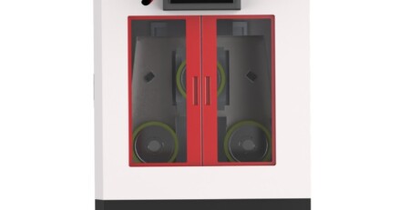
The fundamental components of a diamond wire loop cutting system include:
– Diamond-impregnated wire: Specially engineered wire with industrial diamonds uniformly distributed and bonded to its surface
– Precision guidance system: Sophisticated rollers and tensioning mechanisms that maintain wire stability and alignment
– Advanced control system: Computer Numerical Control (CNC) systems that manage cutting parameters with exceptional accuracy
– Coolant delivery system: Integrated systems that manage temperature and remove debris from the cutting zone
The shift to diamond wire loop technology has been driven primarily by its superior cutting efficiency, reduced kerf loss, and enhanced surface quality compared to traditional methods . These advantages have become increasingly critical as semiconductor manufacturers pursue thinner wafers to maximize yield from expensive semiconductor ingots.
Current Industry Applications and Adoption Trends
Semiconductor Wafer Manufacturing
In semiconductor wafer production, 다이아몬드 와이어 루프 cutting has become the dominant slicing technology for silicon wafers . The technology’s ability to maintain precise control over wafer thickness while minimizing surface damage has made it indispensable for modern fabrication facilities. Particularly for photovoltaic silicon applications, the industry is aggressively pursuing wafer thicknesses below 150 micrometers while simultaneously adopting finer diamond wires with diameters under 35 micrometers to maximize yield per ingot .
Advanced Materials Processing
Beyond conventional silicon, diamond wire loop cutting has proven valuable for processing emerging semiconductor materials:
– 실리콘 카바이드 (원문대로): Essential for power electronics and high-temperature applications
– Gallium Arsenide (가스(GaAs)): Used in high-frequency and optoelectronic devices
– 질화갈륨 (질화 갈륨): Important for RF applications and power electronics
The technology’s adaptability to different material properties has facilitated its adoption across various semiconductor segments, from traditional silicon-based microelectronics to compound semiconductors enabling specialized applications.
Thin Wafer Production
The drive toward thinner wafers represents a significant trend in both photovoltaic and microelectronic applications . For photovoltaics, thinner wafers reduce silicon consumption per watt, directly impacting production costs. In microelectronics, thin wafers enable advanced packaging technologies and three-dimensional integrated circuits. Diamond wire loop cutting has positioned itself as the enabling technology for these industry developments, though not without technical challenges that will be discussed later.
Critical Technological Advantages of Diamond Wire Loop Cutting
Superior Surface Quality and Reduced Kerf Loss
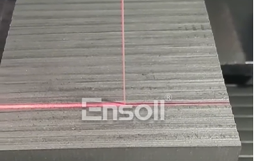
The fixed abrasive nature of diamond wire loop cutting produces exceptional surface quality compared to slurry-based methods. The controlled interaction between diamond particles and the workpiece results in more consistent surface characteristics with reduced subsurface damage. This quality advantage translates directly to downstream benefits, including simplified polishing processes and improved device performance.
또한, 다이아몬드 와이어 루프 create a narrower kerf—the material removed during cutting—than traditional methods. This reduction in kerf width significantly decreases material waste, which is particularly valuable when processing expensive semiconductor-grade crystals. The combination of superior surface quality and reduced kerf loss has established diamond wire loop cutting as the more material-efficient and economically viable option for many semiconductor slicing applications.
Enhanced Processing Efficiency
Diamond wire loop systems offer substantial improvements in cutting speeds and throughput capacity compared to alternative methods. The continuous motion of the diamond-impregnated wire, combined with optimized cooling and debris removal, enables significantly faster processing times. This efficiency advantage has become increasingly important as wafer diameters continue to increase across the semiconductor industry.
The technology also supports greater automation potential than slurry-based systems. The elimination of messy slurries simplifies material handling and reduces cleanup requirements between batches. This characteristic aligns perfectly with the semiconductor industry’s drive toward fully automated fabrication facilities with minimal human intervention.
Environmental and Operational Benefits
The transition to diamond wire loop cutting has delivered notable environmental advantages over traditional methods:
– Reduced chemical consumption: Elimination of slurry-related chemicals
– Improved recyclability: More straightforward recycling of cutting coolants and silicon debris
– Lower energy consumption: Higher cutting efficiency translates to reduced energy per wafer
From an operational perspective, diamond wire systems typically require less maintenance and experience fewer operational interruptions than slurry-based alternatives, contributing to higher overall equipment effectiveness in production environments.
Persistent Challenges and Limitations
Technical Barriers in Thin Wafer Processing
Despite significant advancements, diamond wire loop cutting faces substantial technical challenges when processing ultra-thin wafers. As wafer thickness decreases below 150 마이크로미터, several issues become increasingly problematic :
– Elevated breakage rates: Thin wafers exhibit higher fragility during handling and processing
– Saw mark visibility: Cutting marks with depths of several micrometers can deteriorate device performance
– Warpage issues: Thinner wafers are more prone to warping, creating handling difficulties
These challenges become more pronounced as manufacturers push the boundaries of wafer thinness to maximize material utilization and reduce costs.
Diamond Wire Loop Durability and Cost Concerns
The use of ultra-fine diamond wires (아래 35 micrometers in diameter) introduces challenges related to wire wear and breakage frequency . As wire diameter decreases, maintaining sufficient tensile strength while accommodating diamond particles becomes increasingly difficult. This limitation accelerates wire degradation and potentially compromises sliced wafer quality.
From an economic perspective, the cost balance between wire consumption and yield improvement remains a critical consideration. While finer wires enable thinner cutting and reduced kerf loss, they typically command higher prices and may require more frequent replacement. Manufacturers must carefully optimize this balance to ensure overall cost-effectiveness in their slicing operations.
Material-Specific Limitations
While diamond wire loop cutting excels with many semiconductor materials, it faces limitations with certain emerging substances. Particularly with ultra-hard materials or those with specific crystal structures, achieving optimal cutting parameters remains challenging. 또한, the technology must continuously adapt to new semiconductor formulations developed to address specific performance requirements in advanced electronic devices.
Recent Technological Innovations and Developments
Advances in Diamond Wire Construction
Recent years have witnessed significant innovation in diamond wire technology itself:
– Enhanced diamond distribution: More uniform distribution of diamond particles for consistent cutting performance
– Improved bonding technology: Advanced electroplating techniques that enhance diamond retention
– Specialized wire coatings: Custom formulations that reduce friction and extend wire lifespan
– Increased wire lengths: Standard and custom lengths now reaching up to 2500 meters for continuous operation
These developments have collectively addressed some limitations while maintaining the core advantages of diamond wire loop cutting.
Machine Design and Control System Improvements
Modern diamond wire loop cutting machines incorporate sophisticated features that enhance performance and usability:
– Advanced tension control: Real-time monitoring and adjustment of wire tension
– Vibration damping systems: Isolation technologies that minimize vibration-induced imperfections
– Intelligent parameter adjustment: Adaptive control systems that optimize cutting parameters based on material feedback
– Integrated metrology: On-board measurement systems that enable real-time quality assessment
These machine-level innovations have expanded the operational window for diamond wire loop cutting while improving consistency across diverse production conditions.
Complementary Process Optimizations
Beyond the cutting technology itself, developments in ancillary processes have supported broader adoption of diamond wire looping:
– Enhanced cooling techniques: Advanced coolant formulations and delivery systems
– Improved cleaning methodologies: More effective post-cutting cleaning processes
– Specialized handling solutions: Equipment designed specifically for thin wafers
– In-line monitoring systems: Real-time quality assessment during production
These complementary innovations have helped address some challenges associated with diamond wire loop cutting, particularly regarding thin wafer processing.
Future Outlook and Emerging Trends
Continued Refinement of Existing Technology
The foreseeable future will likely bring continued incremental improvements to diamond wire loop cutting technology. We can anticipate further refinement in:
– Wire durability: Enhanced wire designs that extend operational lifespan
– Cutting precision: Improved accuracy for increasingly demanding applications
– Process integration: Tighter integration with upstream and downstream processes
– Cost reduction: Economies of scale and manufacturing improvements that lower overall system costs
These incremental advances will solidify diamond wire loop cutting’s position as the preferred slicing technology for many semiconductor materials.
Adaptation to New Semiconductor Materials
As the semiconductor industry explores alternative materials to address specific performance requirements, diamond wire loop technology must adapt accordingly. Emerging materials such as diamond semiconductors themselves represent both an opportunity and a challenge for cutting technology . While these materials offer exceptional electrical and thermal properties, their extreme hardness presents unique cutting difficulties that current technology may struggle to address efficiently.
Synergy with Industry Megatrends
Diamond wire loop cutting aligns with several semiconductor industry megatrends:
– 지속 가능성: Reduced material waste and chemical usage support environmental goals
– Miniaturization: Enables thinner wafers for compact electronic devices
– Cost reduction: Higher efficiency and yield contribute to overall cost optimization
– Advanced packaging: Supports emerging packaging technologies requiring thin substrates
This alignment suggests continued relevance for diamond wire loop cutting as these industry trends evolve.
결론
Diamond wire loop cutting has established itself as a critical technology in semiconductor manufacturing, particularly for wafer slicing applications. Its advantages in terms of cutting efficiency, 표면 품질, and material utilization have driven widespread adoption across the industry. 그렇지만, challenges remain, especially regarding thin wafer processing, wire durability, and cost management.
The technology continues to evolve, with ongoing innovations addressing its limitations while enhancing its strengths. As semiconductor materials and requirements diversify, diamond wire loop cutting must adapt to maintain its relevance. The coming years will likely see further refinement of existing approaches alongside potential breakthroughs that could expand the technology’s application range.
반도체 제조업체용, understanding the current state and trajectory of diamond wire loop cutting is essential for making informed decisions about production methodologies. While not a universal solution for all materials and applications, its demonstrated benefits ensure its continued importance in semiconductor manufacturing for the foreseeable future. As with many technologies in the semiconductor ecosystem, the balance between performance, cost, and reliability will ultimately determine its position in the manufacturer’s toolkit.
자주 묻는 질문
How is diamond wire loop used in semiconductor manufacturing?
It slices silicon, 원문대로, and sapphire ingots into wafers with a continuous diamond-coated wire loop, replacing older slurry-based wire saws for better precision and cleanliness.
What advantages does it bring to wafer production?
Narrower kerf (more wafers per ingot), less sub-surface damage (less polishing), and water-based cooling (cleaner process) — together raising yield and lowering cost per wafer.
What are the current challenges of the technology?
Wire wear and life management, stable tension control on very large ingots, and meeting ever-thinner wafer specs without increasing breakage.
Did diamond wire loop replace slurry wire saws?
In most photovoltaic and an increasing share of semiconductor slicing, yes — fixed-diamond wire has largely displaced loose-abrasive slurry sawing because it is faster, cleaner, and more consistent.
엔솔 엔지니어링 팀이 검토한 기술 내용 — 다이아몬드 와이어 루프 제조업체 10+ 다년간의 생산 경험을 가진 회사.