切割碳化硅基板: 技术指南
Introduction to Silicon Carbide Substrate Cutting
- Silicon carbide’s crystal structure and orientation strongly affect cutting behavior; optimizing the cutting direction improves both quality and wire life.
- The main SiC cutting methods — laser, multi-wire saw and diamond wire loop — trade cutting speed against surface damage.
- For SiC substrates, diamond wire loop cutting offers the best balance of surface quality, kerf loss and throughput.
碳化硅 (原文如此) 已成为一种革命性的半导体材料, transforming power electronics and high-temperature applications with its superior properties. The process of 切割碳化硅 substrates represents a critical manufacturing step that directly impacts material utilization, device performance, and production economics. Unlike conventional silicon, SiC’s exceptional hardness and anisotropic crystal structure present unique challenges that demand specialized cutting approaches and precise directional control.
The global SiC substrate market continues to expand rapidly, driven primarily by electric vehicle adoption, 5G infrastructure deployment, and renewable energy technologies. This growth has intensified the focus on optimizing cutting methodologies to maximize yield while maintaining the material’s intrinsic advantages. Understanding the relationship between cutting direction and resulting substrate quality has become increasingly crucial for manufacturers seeking competitive advantage in this dynamic market.
Fundamental Principles of Silicon Carbide Crystal Structure
Crystal Orientation and Anisotropic Properties
Silicon carbide possesses a complex crystalline structure characterized by strong anisotropy across different crystallographic directions. The most common polytypes for electronic applications include 4H-SiC and 6H-SiC, both exhibiting hexagonal crystal symmetry with distinct properties along various axes. This inherent anisotropy means that mechanical, 烫的, and electrical characteristics vary significantly depending on the cutting orientation.
The primary crystallographic directions in SiC include:
– c-axis orientation: Perpendicular to the (0001) basal plane
– a-axis orientation: Parallel to the [11-20] direction
– m-axis orientation: Parallel to the [1-100] direction
Each orientation demonstrates unique characteristics regarding hardness, fracture toughness, and chemical reactivity, directly influencing the selection of optimal cutting parameters and methodologies.
Impact of Crystal Orientation on Material Behavior
The directional dependence of SiC’s properties manifests in several critical aspects:
– Hardness variation: 这 (0001) plane typically exhibits greater resistance to mechanical deformation
– Fracture propagation: Cleavage tendencies differ significantly between crystallographic planes
– Thermal conductivity: Heat dissipation capabilities vary with crystal orientation
– Chemical etching rates: Different planes demonstrate varying susceptibility to chemical processing
Cutting Direction Optimization Strategies
Primary Cutting Orientations and Their Applications
c-Axis Cutting (0001 Plane)
Cutting perpendicular to the c-axis represents the most common orientation for SiC substrate production, particularly for power electronic devices. This orientation provides optimal conditions for subsequent epitaxial growth and facilitates efficient device fabrication. The off-axis cutting technique, 通常 4 degrees toward the [11-20] direction, significantly improves epitaxial layer quality by promoting step-flow growth and reducing defect formation.
Key advantages of c-axis cutting include:
– Superior surface quality for epitaxial readiness
– Reduced defect density in grown layers
– Compatibility with standard device processing
– Established manufacturing protocols
a-Axis Cutting (11-20 Plane)
a-axis cutting has gained prominence for specialized applications requiring enhanced thermal management and specific crystallographic orientations. This orientation demonstrates distinct advantages for vertical power devices and high-frequency applications where thermal dissipation represents a critical performance factor.
Notable benefits of a-axis orientation:
– Improved thermal conductivity in specific directions
– Reduced piezoelectric effects
– Enhanced carrier mobility for certain device architectures
– 高温应用中的卓越性能
碳化硅的先进切割方法
金刚石线环 切割技术
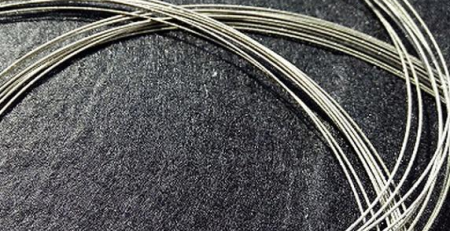
金刚线环切割已成为碳化硅衬底切片的主要技术,因为它能够在保持精确方向控制的同时,将次表面损伤降到最低. 该方法利用连续循环的金刚石线,以受控速度运动,同时维持最佳张力参数.
该工艺在定向切割方面具有多种优势:
– 在整个切割过程中保持精确的方向定位
– 最小的切口损失 (通常 120-200 微米)
– 优良的表面质量,次表面损伤减少
– 衬底厚度均匀性出色
基于激光的切割方法
先进的激光切割技术为特定的碳化硅切割应用提供了互补能力. 超快激光, particularly femtosecond and picosecond systems, enable precise material processing with minimal thermal impact. Stealth dicing techniques, which focus laser energy beneath the substrate surface, offer unique advantages for complex cutting patterns and specific crystallographic orientations.
Key laser cutting benefits include:
– Non-contact processing eliminating mechanical stress
– Flexibility for complex cutting paths
– Minimal material loss through optimized beam control
– Reduced crystal damage through precise energy deposition
Multi-Wire Sawing for High-Volume Production
For high-volume manufacturing environments, multi-wire sawing represents the most efficient approach for directional SiC substrate production. These systems utilize hundreds of parallel diamond wires operating simultaneously to process multiple substrates from a single crystal ingot. Advanced tension control systems and precision guidance mechanisms ensure consistent cutting orientation throughout the production batch.
Factors Influencing Cutting Direction Selection
Device Performance Requirements
The optimal cutting direction depends significantly on the intended device application and performance specifications:
Power Electronics Applications
For MOSFETs and diodes, the standard practice involves 4° off-axis c-plane cutting to optimize:
– Channel mobility and carrier transport
– Gate oxide interface quality
– Breakdown voltage characteristics
– Switching performance parameters
RF and Microwave Devices
High-frequency applications often benefit from alternative orientations that provide:
– Enhanced electron saturation velocity
– Reduced surface state density
– Improved thermal management capabilities
– Superior high-frequency response
Manufacturing Economics and Yield Optimization
Cutting direction significantly impacts production economics through multiple factors:
Material Utilization Efficiency
The relationship between cutting orientation and kerf loss directly affects substrate cost. Optimized directional cutting can improve material utilization by 15-25% compared to non-optimized approaches through:
– Reduced kerf width through directional hardness optimization
– Enhanced cutting speed based on crystallographic orientation
– Improved yield through fracture prevention
Processing Efficiency Considerations
Different cutting directions demonstrate varying processing characteristics:
– Cutting speed variation up to 40% between orientations
– Tool wear rates differing by crystallographic direction
– Surface preparation requirements varying with orientation
– Etching and polishing efficiency depending on crystal plane
定向切割的质量控制与计量
切割前的取向验证
切割前的精确晶体取向评估是关键的质量控制步骤. 先进的 X 射线衍射系统通过以下方式提供微米级的取向精度:
– 高分辨率摇摆曲线分析
– 自动化晶体取向映射
– 实时取向验证
– 缺陷密度评估
过程中的监测与控制
现代切割系统整合了复杂的监测功能以维持定向精度:
– 实时张力和对准监测
– 工艺稳定性的振动分析
– 热管理系统优化
– 定向偏差的自动修正
切割后的质量评估
切割过程后的全面计量确保定向精度和质量:
– 使用原子力显微镜进行表面粗糙度测量
– 通过横截面分析评估亚表面损伤
– 晶体学完整性验证
– 厚度及弯曲/翘曲特性表征
未来趋势 碳化硅 定向切削
先进制造技术
SiC切削技术的发展持续应对新兴挑战:
智能切削系统
下一代切削系统结合了基于人工智能的方向控制优化:
– 用于参数优化的机器学习算法
– 基于传感器反馈的实时自适应控制
– 用于保持一致性能的预测性维护
– 自动化质量评估与校正
混合加工方法
组合方法提供增强能力:
– 用于困难切削方向的激光辅助机械切削
– 用于复杂几何形状的顺序加工
– 闭环控制的集成计量
– 特定应用的多阶段优化
工业 4.0 集成
数字化趋势正在改变碳化硅切割操作:
– 用于工艺模拟的数字孪生技术
– 用于实时监控的物联网连接
– 用于持续改进的数据分析
– 用于质量可追溯的自动报告
结论
碳化硅基板切割方向的优化是最大化器件性能和制造效率的关键因素. 随着碳化硅技术向更大直径发展, 提高的质量, 以及降低成本, 精确方向控制的重要性日益突出.
先进切割方法的结合, 全面的工艺理解, and sophisticated metrology enables manufacturers to achieve new levels of precision and efficiency in SiC substrate production. Future developments in intelligent manufacturing and hybrid processing approaches promise further enhancements in directional cutting capabilities, supporting the continued expansion of silicon carbide across power electronics, RF applications, and emerging technology domains.
Manufacturers who master the complexities of crystallographic orientation and cutting direction optimization will maintain competitive advantage in the rapidly evolving semiconductor landscape, delivering superior substrates that unlock the full potential of silicon carbide technology.
The wider context for substrate work is how to process silicon carbide from ingot through to polished wafer.
常见问题
Why does cutting direction matter for silicon carbide?
SiC is a crystalline material, and its fracture behavior changes with crystal orientation. Choosing the right cutting direction reduces chipping, cracking and wire wear.
What are the main methods for cutting SiC substrates?
激光切割, multi-wire sawing and diamond wire loop sawing. Laser is fastest but thermally damaging; wire-based methods are slower but produce far better surfaces.
Why choose diamond wire loop cutting for SiC substrates?
Its cold abrasive action gives a narrow kerf and minimal sub-surface damage on an extremely hard material, reducing the lapping needed before epitaxy.
技术内容由Ensoll工程团队审核——一家金刚线环制造商 10+ 多年生产经验.