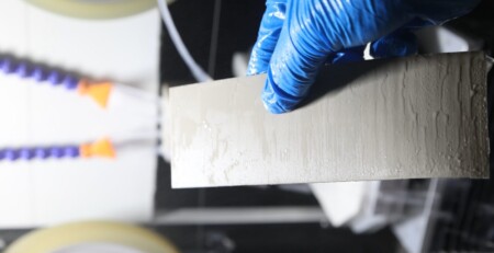
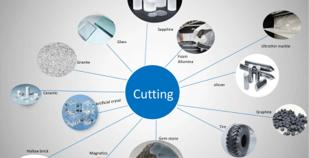
使用钻石线环进行半导体晶体切割
- Semiconductor crystal cutting transforms raw ingots into wafers, 切片步骤决定了产率和后续表面质量.
- Diamond wire loop cutting works by running a diamond-coated wire at high speed under coolant, grinding the crystal with a narrow, controlled kerf.
- Compared with ID blades and slurry saws, diamond wire loop cuts Si, 原文如此, GaN and sapphire with less material loss and lower sub-surface damage.
Introduction to Semiconductor Crystal Cutting
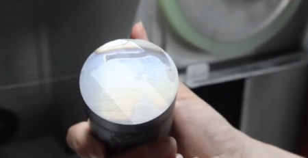
The semiconductor industry relies on precision cutting technologies to transform raw crystal ingots into functional wafers for electronic devices. Among various cutting methods, diamond wire loop technology has emerged as the gold standard for processing advanced semiconductor materials. 这种创新方法在处理如碳化硅这样的挑战性材料时提供了无与伦比的精度 (原文如此) 以及氮化镓 (赣语), 同时在传统硅晶圆上保持高效率.
金刚石线环 切割使用嵌有金刚石颗粒的细小, 柔性线,实现即使是最硬半导体晶体的干净, 精确切割. 该技术通过显著减少材料损耗并提高表面质量,相比传统的基于刀片的方法,已彻底改变了晶圆生产. 随着半导体器件在尺寸上不断缩小,同时要求更高性能, 金刚石线切割提供的精度变得越来越关键.
金刚石线环切割工艺
How 金刚石线环技术 Works
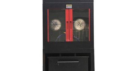
The diamond wire loop system consists of a continuous wire coated with industrial diamond particles running through a series of precision guides. During operation:
- The wire moves at controlled speeds (通常 10-30 米/秒)
- Tension is maintained at optimal levels (通常 15-30 N)
- Cutting fluid is applied to reduce heat and remove debris
- Computer-controlled positioning ensures accurate cuts
This configuration allows for:
→ Uniform material removal
→ Minimal kerf loss
→ Excellent surface finish
→ Reduced subsurface damage
Advantages Over Traditional Cutting Methods
Compared to conventional inner diameter (ID) saws or laser cutting:
- 材料节约: Kerf loss reduced by 50-70%
- 质量改进: Surface roughness improved by 30-50%
- 多面性: Capable of cutting ultra-hard materials like SiC
- Productivity: Multi-wire systems can cut hundreds of wafers simultaneously
- Cost Efficiency: 更长的工具寿命和更低的能耗
切割不同的半导体材料
硅片切割 (单晶 & 多晶)
硅仍然是半导体制造的主力材料, 包括单晶和多晶硅都需要精确切割:
单晶硅:
- 适用于高性能集成电路和太阳能电池
- 金刚线参数:
– 线径: 0.12-0.18 毫米
– 金刚石粒度: 15-25 微米
– 切割速度: 0.5-1.5 毫米/分钟
多晶硅:
- 用于对成本敏感的应用,如太阳能电池板
- 切割注意事项:
– 稍大的金刚石粒度 (20-30 微米)
– 可能实现更高的进给速度
– 对晶体方向的敏感性较低
碳化硅 (原文如此) 加工挑战
 碳化硅由于以下原因具有独特的切割难度:
- 极高的硬度 (莫氏硬度 9.5, 几乎与金刚石一样硬)
- 高脆性
- 高昂的原材料成本 (使材料节约至关重要)
碳化硅的金刚线环解决方案:
- 专用金刚石粘结剂以提高颗粒保持力
- 优化的冷却液配方
- 先进的张力控制系统
- 典型切割速度: 0.3-0.8 毫米/分钟
复合半导体: 砷化镓, 磷化铟 (InP), 和氮化镓 (GaN)
砷化镓 (砷化镓):
- 用于射频和光电子器件
- 切割要求:
– 低张力以防止开裂
– 基于酒精的冷却液
– 中等金刚石颗粒尺寸 (20-30 微米)
磷化铟 (磷化铟 (InP)):
- 对光子应用至关重要
- 加工注意事项:
– 非常低的机械应力切割
– 温控环境
– 超细金刚石颗粒 (10-15 微米)
氮化镓 (赣语):
- 实现下一代功率电子器件
- 切割参数:
– 中等张力设置
– 镍基金刚石涂层线
– 切割速度类似于碳化硅 (SiC)
优化金刚石线圈性能
关键工艺参数
为了达到最佳切割效果, 制造商必须仔细控制:
- 线规范
– 直径 (通常 0.1-0.2 毫米)
– 金刚石颗粒大小 (10-30 微米)
– 结合基体组成
- 操作条件
– 导丝速度 (10-30 米/秒)
– 张力力 (15-30 N)
– 进给速度 (与材料相关)
– 冷却液流量和组成
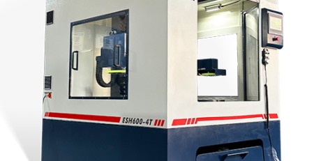
- 机器配置
– Guidance system precision
– Vibration isolation
– Automation features
质量控制措施
Implementing robust QC protocols ensures consistent results:
- 切割前材料检查
- Real-time process monitoring
- Post-cut wafer characterization
– Surface roughness measurements
– Thickness variation analysis
– Subsurface damage evaluation
- 统计过程控制实施
Industry Applications and Case Studies
Solar Photovoltaic Manufacturing
iamond wire cutting has transformed solar cell production:
- 40% reduction in silicon waste
- 30% increase in cutting throughput
- Improved wafer strength for thinner designs
- Case study: Leading PV manufacturer increased yield by 22% after switching to diamond wire
Power Electronics Production
SiC and GaN device manufacturing benefits include:
- Cleaner edges for improved device performance
- Ability to process larger diameter wafers
- Reduced breakage during handling
- Example: EV inverter producer reduced defect rates by 35%
RF and Optoelectronic Components
Precision cutting of GaAs and InP enables:
- Higher frequency device performance
- Improved photonic device efficiency
- Better yield for expensive compound materials
- 应用: 5G RF filter manufacturer achieved 15% cost reduction
Future Trends in Diamond Wire Cutting
Technology Advancements
Emerging innovations include:
- Smart wires with embedded sensors
- AI-driven process optimization
- Nanocomposite diamond coatings
- Dry cutting developments for certain applications
Market Growth Projections
The diamond wire cutting market for semiconductors is expected to:
- Grow at 12.5% CAGR through 2030
- Reach $1.2 billion by 2028
- Expand into new materials like Ga₂O₃
Conclusion and Implementation Guide
Diamond wire loop cutting has become indispensable for modern semiconductor manufacturing. When implementing this technology:
- 材料评估
– Evaluate crystal properties
– Determine quality requirements
– Calculate ROI potential
- System Selection
– Choose appropriate wire specifications
– Select machine capabilities
– Consider automation needs
- Process Development
– Optimize cutting parameters
– Establish QC protocols
– Train operators
- Continuous Improvement
– Monitor performance metrics
– Implement upgrades
– Stay current with technology trends
For semiconductor manufacturers looking to improve yields, 降低成本, and enhance product quality, diamond wire loop cutting offers a proven solution that continues to evolve with the industry’s needs.
Crystal orientation and feed rate matter here for the same reasons they do in cutting silicon wafers, where chipping directly reduces usable area.
常见问题
How does diamond wire loop cutting work for semiconductor crystals?
A closed loop of steel wire coated with diamond abrasive runs continuously at high speed under coolant, micro-grinding the crystal into wafers with a narrow, well-controlled kerf.
What are the advantages of diamond wire loop over traditional cutting methods?
Narrower kerf loss, better surface geometry, no slurry to manage, and far less sub-surface damage than ID blade or slurry sawing.
Can diamond wire loop cut SiC, GaN and sapphire as well as silicon?
是的. Diamond is the hardest abrasive, so the same platform cuts all common semiconductor crystals; only speed, tension and coolant parameters are adjusted per material.
技术内容由Ensoll工程团队审核——一家金刚线环制造商 10+ 多年生产经验.