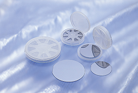
A semiconductor chip, 通常称为集成电路, is a semiconductor device fabricated on a semiconductor wafer through processes such as etching, wiring, and patterning to achieve specific functions. Beyond silicon chips, common semiconductor materials include gallium arsenide, 氮化镓, 和碳化硅.
最后审核: 九月 2026
关键要点
Semiconductors are materials with conductivity between conductors and insulators, forming the basis of all integrated circuits.
Beyond silicon, key semiconductor types include gallium arsenide (砷化镓), 氮化镓 (赣语) 和碳化硅 (原文如此), each with distinct application niches.
GaAs serves RF and optoelectronics, GaN serves high-frequency power, and SiC serves high-voltage, high-temperature power devices.
半导体制造过程类似于将基础材料变成黄金, 主要涉及对硅片的一系列处理. 基本上, 通过外延生长, 光刻, 蚀刻, 掺杂, 和抛光, the required circuits are formed on the silicon wafer, transforming it into a chip.
Types of Semiconductors
Semiconductor materials are electronic materials used in the production of semiconductor devices and integrated circuits, forming the foundation of the semiconductor industry.
With the emergence of new semiconductor materials, advancements in power electronics technology, and improvements in manufacturing processes, semiconductors have undergone three generations of changes. Gallium arsenide (砷化镓) and gallium nitride (赣语), as well as silicon carbide (原文如此) 半导体, represent the second and third generations of semiconductors, 分别.
Compared to the first-generation semiconductor silicon (四), these materials exhibit superior performance in aspects such as high frequency and high temperature.
Compound semiconductor chips, known for their excellent high-frequency performance, are commonly used in the production of power semiconductors, with their applications becoming increasingly widespread. Through techniques such as frequency conversion, voltage transformation, current modulation, power amplification, and management, 这些芯片主要有两个功能: 放大和开关.
砷化镓半导体芯片主要用于微波功率器件, which operate in the microwave frequency range (between 300 和 300,000 megahertz). Due to the inherent physical limitations of silicon (四), it can only be applied at frequencies below 1 GHz. 然而, 近年来, the rapid development of wireless high-frequency communication products has propelled gallium arsenide to the forefront, showcasing characteristics such as high operating frequencies, electron mobility rates, resistance to natural radiation, and low power consumption, making it widely used in the field of microwave communication.
Given the high-frequency transmission characteristics of gallium arsenide, it has seen rapid growth not only in mobile phone applications but also in WiFi modules embedded in laptops, tablets, fixed network wireless transmission, as well as fiber optic communication, satellite communication, point-to-point microwave communication, cable television, automotive navigation systems, and collision avoidance systems. These applications often employ varying numbers of power amplifiers (ranging from 1 自 4 chips), driving the significant advancement of gallium arsenide.
Gallium Nitride Semiconductor
Gallium nitride material, with a bandgap width of 3.4 eV, is considered a third-generation semiconductor material along with materials like SiC and diamond, known as wide-bandgap semiconductors. Due to its advantages such as a wide bandgap, high breakdown field, large saturation electron velocity, 高导热性, 低介电常数, 化学稳定性, and strong radiation resistance, gallium nitride has become one of the preferred materials for high-temperature, high-frequency, 和大功率微波设备.
Comparison of Gallium Nitride (赣语) with Gallium Arsenide (砷化镓) and Silicon (四):
The increasing demand for high-speed, high-temperature, and high-power semiconductor devices has led to the gradual adoption of gallium nitride material in the semiconductor market. Its primary application areas include:
Renewable Energy Sector:
In the field of renewable energy, gallium nitride plays an extremely important role in integrating wind and solar power into the grid and reducing transmission losses. Green energy, 电动汽车, green electronic lighting, and other emerging areas are becoming new hotspots for power device market applications, with strong demand.
Information Communication Equipment Sector:
Enhanced gallium nitride transistors exhibit high radiation resistance, making them suitable for power and communication systems in communication and scientific satellites. Point-to-point communication, satellite communication, various radars, and new industrial/defense applications will benefit from the application of these high-power gallium nitride devices.
4C Industries:
Major domestic IT products are expected to maintain strong market demand, with traditional products like laptops, monitors, printers, televisions, home theater systems, and Blu-ray players, as well as emerging automotive electronics, projected to experience steady growth in the future. As production capacity for electronic products such as air conditioners and energy-efficient motors shifts to the Chinese mainland, the demand for power semiconductors is expected to double.
Smart Grid Sector:
Power semiconductors play a crucial role in improving the overall energy efficiency of the entire power supply chain—from generation, transmission, and distribution to end-user consumption—in the field of smart grids.
Silicon Carbide Semiconductor
碳化硅 (原文如此) has become one of the most prominent semiconductor materials due to its outstanding performance under high temperature, 高压, and high frequency conditions. It is widely used in power conversion devices such as AC-DC converters and is expected to gradually replace silicon comprehensively in the field of semiconductor power devices, heralding the dawn of the Silicon Carbide Semiconductor era.
Compared to silicon devices, SiC semiconductor chips can reduce power losses by nearly 50%, effectively enhancing power conversion efficiency. SiC devices, with their high conversion efficiency and low heat generation, can reduce the size of cooling systems, leading to overall downsizing of power conversion devices. 这对于像新能源汽车这样需要大量电力转换装置的系统具有重要意义. 因此, 对于需要高转换效率和功率密度的系统, 碳化硅器件提供了无与伦比的优势,是首选.
半导体制造工艺类似于将铅变成金, 主要涉及对硅片的一系列处理. 虽然详细解释可能非常复杂, 简单来说, 它涉及外延生长, 光刻, 蚀刻, 掺杂, 以及抛光以在硅片上创建所需的电路, transforming it into a chip. Steps like photolithography and etching still rely on foreign technologies and the use of foreign patents
Semiconductor processing methods
Four Cutting Technologies: A Comparative Overview:
1. 金刚石线环切割
Principle: A fast-moving loop of wire, coated with diamond particles, acts as a cutting tool, grinding through the material. Coolant is often used.
Key Advantage:Low stress, 高精度, minimal material waste. 这 “flexible” wire is gentle on brittle materials, enabling clean cuts with almost no edge chipping. It is the preferred method for slicing high-value, hard, brittle materials like SiC, 赣语, 蓝宝石, 和 光学玻璃into thin wafers.
Limitation:Limited cutting speed. As a grinding process, its material removal rate is slower than thermal methods like laser cutting, making it less efficient for high-volume or rough cutting jobs.
2. Diamond Saw Blade Cutting
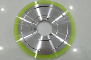
Principle:A rotating circular blade with a diamond-coated edge cuts through the material, similar to a precision stone cutter.
Key Advantage:Proven technology, 高效率, relatively low cost. It’s the standard method for rough cutting and sizing blocks of silicon and ceramic.
Limitation:High mechanical impact. It can easily cause edge chipping and internal stress or micro-cracks, making it unsuitable for finishing ultra-thin, ultra-hard, or high-value materials.
3. 激光切割
Principle:A focused, high-energy laser beam melts, vaporizes, or alters the material, with a gas jet removing the debris.
Key Advantage:Non-contact, no tool wear, very fast, highly flexible. It easily handles complex 2D shapes and can perform “stealth dicing” (separation via internal modification), making it ideal for wafer dicing and shaping silicon, 蓝宝石, 和玻璃.
Limitation:Creates a heat-affected zone that may change material properties at the cut edge. It can struggle with highly reflective (例如, pure copper) or transparent materials. Equipment is expensive.
4. Electrical Discharge Cutting (电火花线切割)
Principle:Controlled spark discharges between a thin wire electrode and the workpiece generate intense heat, locally melting and vaporizing the material.
Key Advantage:Cuts any conductive material regardless of hardness (例如, hardened steel, 碳化钨, conductive ceramics). It achieves very high precision and can create complex shapes.
Limitation:Only works on conductive materials. 过程缓慢, and it leaves a recast layer on the cut surface.
Summary & Selection Guide
There is no single “best” technology—each is most suitable for specific tasks:
For ultimate cut quality and minimal loss when slicing hard, brittle wafers (例如, 原文如此): Choose金刚石线环 切削.
For efficient, low-cost rough cutting of hard, brittle blocks: Choose Diamond Saw Blade Cutting.
For high-speed cutting of complex 2D shapes in various materials (including non-metals): Choose Laser Cutting.
For machining intricate shapes in very hard, conductive materials (例如, molds): Electrical Discharge Cutting is the only choice.
Current Situation:
现在, many technologies require a fresher perspective to be infused, as each step in the process could potentially lead to significant advancements. Regarding one specific aspect, we conducted a experiment on cutting 12-inch ingots two weeks ago. We utilizedEnsolltools工具Limited’s金刚石线锯 科技, where the wire marks are nearly invisible, and the flatness can be controlled within 3 微米. This method addresses many issues related to cutting semiconductor concave surfaces, greatly reducing the difficulty of subsequent polishing and material consumption.
A semiconductor is a material whose electrical conductivity sits between a conductor and an insulator and can be controlled by doping, making it the foundation of integrated circuits.
What are the main types of semiconductor materials?
Silicon dominates general ICs; compound semiconductors include gallium arsenide (RF, optoelectronics), 氮化镓 (high-frequency power) 和碳化硅 (高压, high-temperature power).
Where are SiC and GaN semiconductors used?
SiC is used in EV inverters and high-voltage power modules, while GaN is used in fast chargers, RF power amplifiers and 5G infrastructure.